5.1.2.2. Digital Output
5.1.2.2. Digital Output
The following Figure and Table show the pin composition of terminal block (TB01~4) for digital output. Each terminal block can be connected to 8 output signals, and different power can be used depending on the usage.

Figure 5.4 Pin Configuration of Digital Input/Output Terminal Block of the Public IO Board(BD580)
Table 5‑2 Pin Configuration of Digital Input/Output Terminal Block (TBOn*) of the Public IO Board (BD580)
Pin Number | Signal Name | Signal Description |
10 | COMn* | COMMON power (Ground DC24V or DC24V) |
9 | ||
8 | DOn*1 | 1st output of nth public output signal port of user |
7 | DOn*2 | 2nd output of nth public output signal port of user |
6 | DOn*3 | 3rd output of nth public output signal port of user |
5 | DOn*4 | 4th output of nth public output signal port of user |
4 | DOn*5 | 5th output of nth public output signal port of user |
3 | DOn*6 | 6th output of nth public output signal port of user |
2 | DOn*7 | 7th output of nth public output signal port of user |
1 | DOn*8 | 8th output of nth public output signal port of user |
Note *) Terminal Block Number n = 1~4 (Ex, TBO1, TBO2, TBO3, TBO4)
The output specification of each port is as follows.
l Output component: Photo MOSFET output
l Rated output: 125mA (Continuous load current) / 24V DC
l Common power: Ground 24VDC or 24VDC
The user connects the output signal through the method shown in Figure 5.5 below. First, connect the common signal (COMMON) to the public IO board (BD580), and then connect each signal to the output pin according to the usage. For the power, 8 output signals can be composed as a unit and can be used differently.
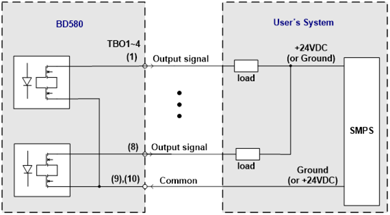
Figure 5.5 Method for the Connection of the Output Signals of the Public IO Board (BD580)