1.2. Hi5 Robot controller’s Modbus function
1.2. Hi5 Robot controller’s Modbus function
Hi5 Robot controller only supports the slave function of Modbus.
(1) MODBUS transmit mode
n ASCII mode
n RTU(binary) mode
(2) Supporting function
n 01: read coils (bits)
n 02: read discrete inputs (bits)
n 03: read holding registers (multiple)
n 04: read input registers (multiple)
n 05: write single coil (bit)
n 06: write single holding register
n 15: write coils (multiple bits)
n 16: write holding registers (multiple)
(3) Slave address setting
n Slave address: 1~247
n When command’s slave address is 0, broadcasting function that activates all slaves regardless of the configured address is supported.
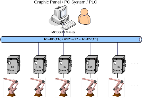
(4) Communication media
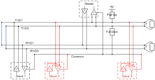
n CNSIO: RS232/RS422/RS485 selective use → 1:1(RS232/RS422), 1:N(RS485)
① RS232C’s pin array: No.2(TxD), 3(RxD), 5(GND) → Use PC and direct cable
② RS422/RS485’s pin array: 1(Tx), 6(/Tx), 4(Rx), 9(/Rx)
n OPSIO: RS232/RS422/RS485 selective use → 1:1(RS232/RS422), 1:N(RS485)
RS232C’s pin array: No.3 (TxD), 2(RxD), 5(GND) → Use PC and cross cable
RS422/RS485’s pin array: 1(Tx), 6(/Tx), 4(Rx), 9(/Rx)
(5) Use condition
n TO use embedded PLC’s Relay as MODBUS function, embedded PLC must be at Run status. (Note:Hi5’s PLC enable can be configured at TP)
n PLC’s operation mode setting can be configured at TP 『[F7]: Cnd. set』→ 『[F1]: App. cnd』as below
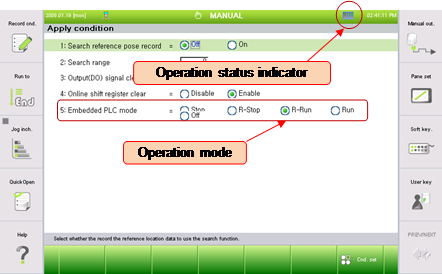
n If embedded PLC is disabled, Write on embedded PLC’s Relay is not supported. However, read from all register or coil is still doable
(6) Example of MODBUS virtual management
n Operator function:
A robot of Low cost GP (Graphic Panel) or few robots that support Serial MODBUS can be connected with RS232/RS422/RS485 to use
n PLC communication:
Communication with PLC that has MODBUD Master function can be provided as a low cost solution
n PC Robot management system:
Robot management system that monitors or manages I/O signal of robot by using PC serial port can be constructed
(7) Hi5 Relay mapping
Modbus Data Model |
| Relay mapping: Refer to Hi5 relay configuration & IO data flow | Function | |
| 1bit | |||
Relay name | Register | Logical Add. | ||
Input Discrete Add: 0x0000~0xffff Quantity: 1~2039(bit)
Input Registers Add: 0x0000~0xffff Quantity: 1~127 | External Input | X1~8192 | 0x0001~0x2000 | Read Function 02: read discrete Inputs (bits) 04: read input registers (multiple) |
PLC Input | DO1~4096 | 0x2001~0x3000 | ||
Fieldbus In #1 | FB1.X1~960 | 0x3001~0x33C0 | ||
~~Fieldbus In #2~~ | ~~FB2.X1~960~~ | ~~0x3401~0x37C0~~ | ||
Fieldbus In #3 | FB3.X1~960 | 0x3801~0x3BC0 | ||
~~Fieldbus In #4~~ | ~~FB4.X1~960~~ | 0x3C01~0x3FC0 | ||
CC-Link In | FB5.X1~256 | 0x4001~0x4100 | ||
Fieldbus Node In | FN1~64.X1~128 | 0x5001~0x8F80 | ||
Timer | T1~256 | 0xF001~0xF100 | ||
Counter | C1~256 | 0xF201~0xF300 | ||
Analog In |
|
| 1000 magnification Data (ex, 6250→6.250) | |
Add: 0x0000~0xffff Quantity: 1~2039(bit)
Holding Registers Add: 0x0000~0xffff Quantity: 1~127 | External Out | Y1~8192 | 0x0001~0x2000 | Read Function 01: read coils (bits) 03: read holding registers (multiple)
Write Function 05: write single coil (bit) 15: write coils (multiple bits) 06: write single holding register 16: write holding registers (multiple)
AO: 1000 magnification Data (Range: ±12.000) System Memory is reserved |
PLC Out | DI1~4096 | 0x2001~0x3000 | ||
Fieldbus Out #1 | FB1.Y1~960 | 0x3001~0x33C0 | ||
~~Fieldbus Out #2~~ | ~~FB2.Y1~960~~ | ~~0x3401~0x37C0~~ | ||
Fieldbus Out #3 | FB3.Y1~960 | 0x3801~0x3BC0 | ||
~~Fieldbus Out #4~~ | ~~FB4.Y1~960~~ | ~~0x3C01~0x3FC0~~ | ||
CC-Link Out | FB5.Y1~256 | 0x4001~0x4100 | ||
Fieldbus Node Out | FN1~64.Y1~128 | 0x5001~0x8F80 | ||
Special | SP1~128 | 0x9101~0x9180 | ||
Auxiliary | R1~1024 | 0x9201~0x9600 | ||
Keep | K1~1024 | 0x9801~0x9C00 | ||
Timer |
|
| ||
Counter |
|
| ||
Analog Out |
|
| ||
System Memory | SW1~512.1~16 | 0xA001~0xC000 | ||
Shared Registers | Data Memory | MW1~1000.1~16 | 0xC001~0xFE80 | |
HRBASIC | V% variable |
|
| |
RN Register |
|
| Data range: 0~255 | |
V$ variable |
|
| 36 bytes/V$ → 40 x 36/2 = 720 | |
| V! variable |
|
| IEEE single-precision 32bit float point |


Modbus Data Model |
| Relay mapping: Refer to Hi5 relay configuration & IO data flow | Function | ||||
| Register Prefix Name |
| |||||
Relay name | 8bit | 16bit | 32bit | Float(32bit) | Logical Add. | ||
Input Discrete Add: 0x0000~0xffff Quantity: 1~2039(bit)
Input Registers Add: 0x0000~0xffff Quantity: 1~127 | External Input | XB1~1024 | XW1~512 | XL1~256 | XF1~256 | 0x0001~0x0200 | Read Function 02: read discrete Inputs (bits) 04: read input registers (multiple) |
PLC Input | DOB1~512 | DOW1~256 | DOL1~128 | DOF1~128 | 0x2001~0x2100 | ||
Fieldbus In #1 | FB1.XB1~120 | FB1.XW1~60 | FB1,XL1~30 | FB1.XF1~30 | 0x3001~0x303C | ||
~~Fieldbus In #2~~ | ~~FB2.XB1~120~~ | ~~FB2.XW1~60~~ | ~~FB2,XL1~30~~ | ~~FB2.XF1~30~~ | ~~0x3401~0x343C~~ | ||
Fieldbus In #3 | FB3.XB1~120 | FB3.XW1~60 | FB3,XL1~30 | FB3.XF1~30 | 0x3801~0x383C | ||
~~Fieldbus In #4~~ | ~~FB4.XB1~120~~ | ~~FB4.XW1~60~~ | ~~FB4,XL1~30~~ | ~~FB4.XF1~30~~ | ~~0x3C01~0x3C3C~~ | ||
CC-Link In | FB5.XB1~32 | FB5.XW1~16 | FB5,XL1~8 | FB5.XF1~8 | 0x4001~0x4010 | ||
Fieldbus Node In | FN1~64.XB1~16 | FN1~64.XW1~8 | FN1~64.XL1~4 | FN1~64.XF1~4 | 0x5001~0x8F08 | ||
Timer |
|
|
|
|
| ||
Counter |
|
|
|
|
| ||
Analog In |
| AI1~32 |
|
| 0x9A01~0x9A20 | 1000 magnification Data(ex, 6250→6.250) | |
Coils Add: 0x0000~0xffff Quantity: 1~2039(bit)
Holding Registers Add: 0x0000~0xffff Quantity: 1~127 | External Out | YB1~1024 | YW1~512 | YL1~256 | YF1~256 | 0x0001~0x0200 | Read Function 01: read coils (bits) 03: read holding registers (multiple)
Write Function 05: write single coil (bit) 15: write coils (multiple bits) 06: write single holding register 16: write holding registers (multiple)
AO: 1000 magnification Data(Range: ±12.000) System Memory is reserved |
PLC Out | DIB1~512 | DIW1~256 | DIL1~128 | DIF1~128 | 0x2001~0x2100 | ||
Fieldbus Out #1 | FB1.YB1~120 | FB1.YW1~60 | FB1,YL1~30 | FB1.YF1~30 | 0x3001~0x303C | ||
~~Fieldbus Out #2~~ | ~~FB2.YB1~120~~ | ~~FB2.YW1~60~~ | ~~FB2,YL1~30~~ | ~~FB2.YF1~30~~ | ~~0x3401~0x343C~~ | ||
Fieldbus Out #3 | FB3.YB1~120 | FB3.YW1~60 | FB3,YL1~30 | FB3.YF1~30 | 0x3801~0x383C | ||
~~Fieldbus Out #4~~ | ~~FB4.YB1~120~~ | ~~FB4.YW1~60~~ | ~~FB4,YL1~30~~ | ~~FB4.YF1~30~~ | ~~0x3C01~0x3C3C~~ | ||
CC-Link Out | FB5.YB1~32 | FB5.YW1~16 | FB5,YL1~8 | FB5.YF1~8 | 0x4001~0x4010 | ||
Fieldbus Node Out | FN1~64.YB1~16 | FN1~64.YW1~8 | FN1~64.YL1~4 | FN1~64.YF1~4 | 0x5001~0x8F08 | ||
Special | SPB1~16 | SPW1~8 | SPL1~4 | SPF1~4 | 0x9001~0x9008 | ||
Auxiliary | RB1~128 | RW1~64 | RL1~32 | RF1~32 | 0x9101~0x9140 | ||
Keep | KB1~128 | KW1~64 | KL1~32 | KF1~32 | 0x9201~0x9240 | ||
Timer | TB1~1024 | TW1~512 | TL1~256 | TF1~256 | 0x9301~0x9500 | ||
Counter | CB1~1024 | CW1~512 | CL1~256 | CF1~256 | 0x9701~0x9900 | ||
Analog Out |
| AO1~32 |
|
| 0x9A01~0x9A20 | ||
System Memory | SB1~1024 | SW1~512 | SL1~256 | SF1~256 | 0xA001~0xA200 | ||
Shared Registers | Data Memory | MB1~2000 | MW1~1000 | ML1~500 | MF1~500 | 0xA401~0xA7E8 | |
HRBASIC | V% variable |
| V%[1~400] |
|
| 0xB001~0xB190 | |
RN Register |
| RN1~16 |
|
| 0xC001~0xC010 | Data range: 0~255 | |
V$ variable | V$[1~40] | 0xD001~0xD2D0 | 36 bytes/V$ → 40 x 36/2 = 720 | ||||
| V! variable |
|
|
| V![1~400] | 0xE001~0xE320 | IEEE single-precision 32bit float point |


n The italic large numbers from above table are the relay group that used by Modbus.
n Data type: Float type uses IEEE single-precision 32bit float point, 8bit/16bit/32bit use all signed integers(except RN Register), for8bit type, read only according to GP
n Relay’s Endian uses Little Endian;
Example, in case when Float type YF1=6.515625(0x40D08000),
YL1=0x40D08000 → YW1=0x8000, YW2=0x40D0 → YB1=0x00, YB2=0x80, YB3=0xD0, YB4=0x40
Note) Modbus transmit is 16 bit align’s Big Endian. In other word, above transmission will occur in order of 0x80, 0x00, 0x40, 0xD0
n Hi4acontrast changes
L(long)type and F(Float)type that are 31Bit type were added, number of AI/AO expanded (4→32), number of SP/SPB/SPW/SPL/SPF expanded(SPW: 2→8), number of SB/SW/SL /SF expanded(SW: 256→512), size of MB/MW/ML/MF reduced(MW: 5000→1000)
Timer(Tn) and Counter(Cn)’s bit number has expanded(16bit→32bit); Cf) Tn(Cn) and TLn (CLn)’s relationship: If the value of TLn(CLn) is 0, Tn(Cn)=1(activation), if TLn(CLn) is not 0, then Tn(Cn) is 0.
DI/DO, X/Y relay expansion: DI/DO1~256 → 1~4096, X/Y1~256 → 1~8192
Quantity expansion: Bit=2000→2039, Reg=125→127
n Fieldbus Node In/Out: Address: For upper byte, Node number (1~64:0x50~0x8F, offset: 0x50) is assigned, for lower byte, address (bit: 1~128, word: 1~8) is assigned.
Ex,
FN1.X1~128: 0x5001~0x5080, FN2.X1~128: 0x5101~0x5180, FN3.X1~128: 0x5201~0x5280, FN4.X1~128: 0x5301~0x5380, ……, FN64.X1~128: 0x8F01~0x8F80
Ex,
FN1.XW1~8: 0x5001~0x5008, FN2.XW1~8: 0x5101~0x5108, FN3.XW1~8: 0x5201~0x5208, FN4.XW1~8: 0x5301~0x5308, ……, FN64.XW1~8: 0x8F01~0x8F08
(8) Hi5 controller’s relay structure
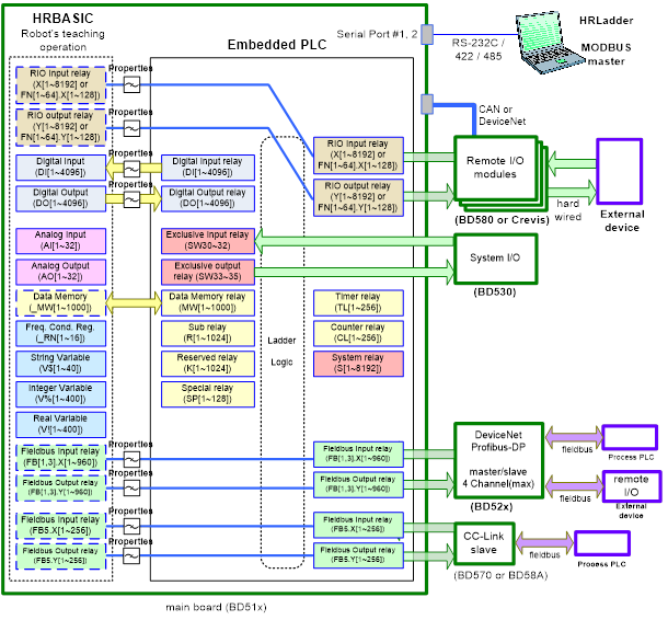
(9) Hi5 controller’s I/O data flow
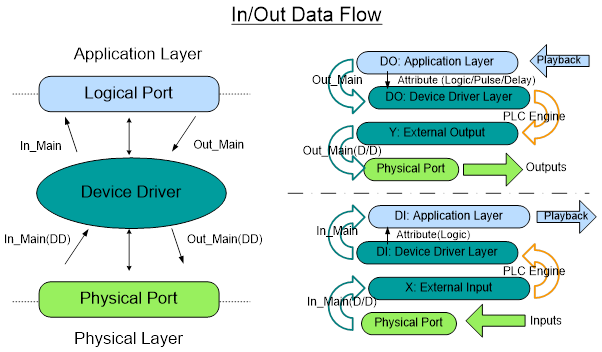
Application layer reads DI from HRBasic, or writes value on D0. Device layer reads D0 output. DI/D0’s device driver layer reads and writes from PLC, I/O monitoring, or Modbus. So there may be some differences between the two according to the properties (logic/pulse/delay)